
Now that we understand the basics of wired communications let’s see the most common standards that you will work with on a peripheral level.
Different goals require different communication standards. A communication which works great between ICs on your PCB are not the best to communicate between computers that are miles away. Speed, power, overhead, voltage levels, etc – these are all factors you need to take into consideration.
What is Peripheral Communications?
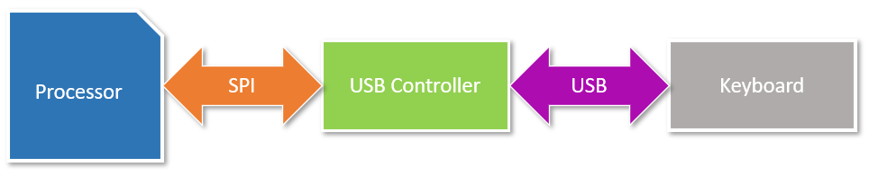
You might have already heard that there are so called Peripheral Controllers in you computer. Do you know what they do? Let’s take the example of inputs from a keyboard. Imagine that when writing a computer program you had to check if a button was pressed, the status of the Caps Lock, if multiple buttons are pressed at the same time, which one was pressed first, etc.. in each iteration. Sounds like a nightmare right? You expect this information just to simply come from your OS and process what you get. Well guess what, your OS/processor wants to outsource this too and have multiple autonomous units on your motherboard that should tell your OS/processor if something interesting happened so they can process it.
The same thing applies to your arduino, raspberry, esp8266.. devices when you connect an add-on board. Would you like to interface with an RFID reader IC on a digital pin level and set everything on a completely low level? No. You expect to have a unit that can be easily connected to your main unit and do some configuration then read the RFID tag itself. So the RFID reader add-on board is a Peripheral Device, it has some intelligence so the data from the RFID reader IC is transferred over a Communications Interface and your Main Unit can accept that interface.
Characteristics
- Typically Peripheral Communication happens on short distances, either on the same PCB or via short wires. SPI for example would not be able to transfer data from your RFID reader in your garden into your raspberry in the house.
- It is often required to be able to connect multiple devices to the same interface/wires in a way that they can be still individually accessed and they are not interfering with each other.
- Depending on the actual interface the list of connected devices might or might not change while the system is running.
- Due to these factors the Peripheral Communications are considered to be quite protected forms of communication and thus the overhead is usually minimized (overhead used for error correction and such).
Peripheral communication is often chained together as communications needs to happen between the processor and the peripheral controller, and between the peripheral controller and the processor.
Now let’s see two of the most common protocols.
Serial Peripheral Interface (SPI)
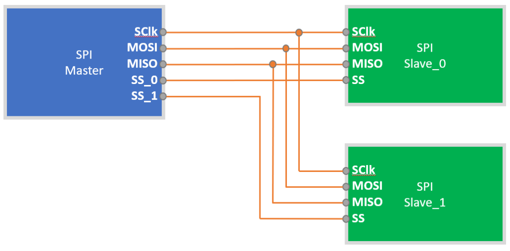
An SPI communication network consists of one Master and one or more Slave devices, the information exchange is a serial type. The Master is responsible for generating the Clock signal and assigning which Slave should be active so it is controlling the communication in general.
The meaning of the signals:
- SClk – Serial Clock
- MOSI – Master Output Slave Input
- MISO – Master Input Slave Output
- SS – Slave Select. Each Slave needs a separate SS signal thus the Master has at least as many SS outputs as many Slave are present
SPI communications happens on low voltage level signals such as 5V or 3.3V.
Communication Process

- The Master tells its slaves which one should listen – this is done by assigning the appropriate Slave Select signal. In most cases a Low value means active.
- The Master then starts the Serial Clock. All devices (Master and Slaves) transmit and receive based on this clock.
- MOSI is the signal where the Master sends data to the Slaves
- MISO is the signal where the selected Slave sends data to the Master
- When the communication is over the Master stops the Serial Clock and removes the Slave Select signal.
This sounds pretty easy so why is it complicated to setup the communication properly? Because for all the devices to communicate properly we need to make sure they speak the “same language”. As there are many parameters for an actual SPI communication, there are also many combination of parameters that won’t work well. Here is what you need to set properly:
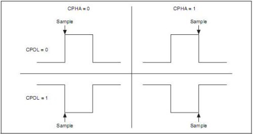
- CPOL – This parameter sets the polarity of the Serial Clock signal.
- CPOL=0 means that the Clock starts in Low and then is raised to High.
- CPOL=1 means that the Clock starts High and is then changed to Low.
- CPHA – This parameters sets the Phase of the Serial Clock signal.
- CPHA=0 means that the data sample should be taken on the First Edge of the Clock.
- CPHA=1 means that the data is sampled on the Second Edge of the Clock.
- SS – However in most cases a Low state means Active some devices use High as a signal for Active state
- Data Length – Your device should now how many data bits are expected.
Overview
As the selection of Slave Devices happens via dedicated Slave Select wires we do not need to do addressing in the Data Signals and such. This simplifies the communication and reduces overhead. At the same time the dedicated Slave Select signals mean additional wires in our setup. We neither have flow control or acknowledge methods.
The dedicated MISO and MOSI signals enable full-duplex (to- and from the Master at the same time) communication between the Master and Slave devices which also improves the communication performance.
Note that most devices (like microcontrollers) have dedicated SPI communication pins, the Slave Select can be usually freely changed though. Of course you can implement SPI communications on any pins with a custom program but then everything is software timed.
Inter-Integrated Circuit (I2C)
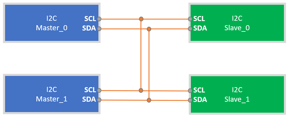
An I2C communication network consists of one or more Master and one or more Slave devices, the information exchange is a serial type. Any Master can generate a Clock signal but first they need to make sure there is no other ongoing communication that they would interrupt.
- SCL is the Serial Clock
- SDA is the Serial Data line
I2C communications happens on low voltage level signals such as 5V or 3.3V.
As you noticed there is no Slave Select, neither two separate Data lines for the two communication direction so there are a few tricks to make this work.
- Start and End of Communication
- Start is signaled by lowering the Data Line and then the Clock going also low
- End is signaled by raising the Clock and then the Data line
- Addressing
- We discussed that there are no Slave Select lines so we need to address the Slave in a communication frame. By default a 7 bit long field is used for addressing, however it can be extended to 10 bits.
- Read or Write
- A Slave cannot initiate a data transfer so the Master can start a communication by selecting the Slave’s address and using a Read/Write bit to indicate if it expects the Slave to transmit data in the upcoming part of the communication.
- Acknowledge
- The receiving party is expected to set the Acknowledge bit after each received 8 bits.
- Flow Control
- However the Master controls the Clock the Slave can keep it in the low state (Clock Stretching) to indicate it needs some time before continuing.
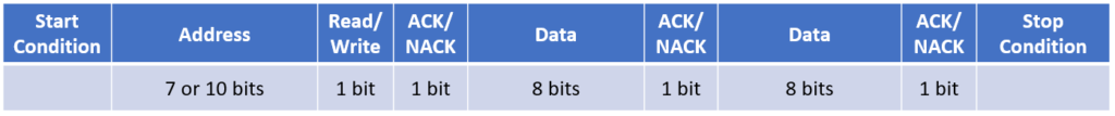
The number of Data Bytes varies, it is not fixed by the I2C standard.


A Read and Write operation is very similar as a waveform – the difference is that:
- Master Writes: the Master starts and ends the frame, also sends the Data bytes and the Slave acknowledges
- Master Reads: the Master starts and ends the frame, the Slave sends the Data bytes and the Master acknowledges
Overview
The I2C communication standard is defined over 2 wires and this can simplify the network setup. Also multiple Masters and multiple Slaves can be present. This flexibility is provided with the trade-off on performance. The I2C protocol is generally slower than the SPI standard and also contains more overhead.
Universal Asynchronous Receiver/Transmitter (UART)
UART is a serial communication method where there is no dedicated clock channel, but the transmitting and receiving parties know in advance the baud rates in order to be able to code and decode the messages. UART uses a special frame format so the beginning and the end of a message can be identified.
The basics of the UART communication is a Serializer – Deserializer architecture.
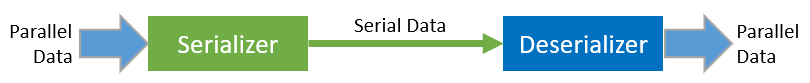
This architecture takes parallel data (5..9 bits for UART), transmit as serial data over one wire (+ the ground), with all the benefits of serial communication. The other side receives the serial data and converts it back to 8 parallel bits.
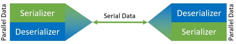
Of course we want full-duplex communication (can receive and transmit at the same time) so both endpoints have a Serializer and Deserializer units that have dedicated Transmit (Tx) and Receive (Rx) channels and the communication happens over two wires (+ ground).
As mentioned UART uses a special framing to be able to properly align with communication frames.
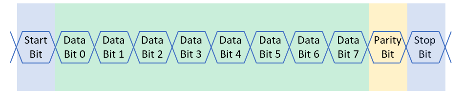
- Start Bit: marks the beginning of a frame, 1 bit long
- Data Bits: also called the payload, carries the actual information. Can be 5..9 bits in the UART standard. 8 is a common value.
- Parity Bit: can be Odd or Even, marks the number of 1’s in the Data Bits. If Even is used then a 1 in this field means even amount of 1’s. If Odd is used then 1 mark odd amount of 1’s. This field is used as a basic error detection:
- The Sender party calculated the parity bit for the payload and appends it into the communication frame
- The receiving party recalculates the Parity on the payload and compares it with the received Parity Bit
- If the Received and Recalculated Parity bits are not a match it means at least one of the received Data Bits is incorrect and the transmission need to be repeated. UART is not capable of correcting errors, however there are other methods that can do that.
- The Parity Bit can be Odd, Even or not used.
- Stop Bit: marks the end of the UART communication frame. Can be 1..2 bits long, 1 bit is the common length.
There is some confusion on the internet about voltage levels associated with UART. UART itself is a way of sending data, a communication method and it does not define a voltage levels. There are various chips that implement UART on various voltage levels (like RS232 @12V). Nevertheless you will find UART written on various devices and in those cases it usually means 3.3V or 5V levels.
Now that we understand how devices communicate in a close vicinity of each other let’s see how devices communicate over larger distances.